数字ASIC设计概要:Tap Cell
标签:
asic

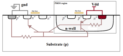
N Well和P-Substrate形成了一个PN结,为了避免这个PN结被正向偏置(Forwad Bias),最容易的办法是把N-Well连接到最高电压上,同时把P-Substrate连接到最低电压上。为了这个目的的连接被称做Well Ties和Substrate Ties,有时也叫做Well Contacts或才Substrate Contacts。
如果上面提到的PN结被导通的话,很可能会形成Latch-Up效应,从而损坏整个芯片。
在《集成电路版图甚础》里这样形容Well Ties和Substrate Ties:
- Rule of Thumb: There is no such thing as too many tie-downs.
- Rule of Thumb: Wherever there is any spare space in an N well, put in a well tie. Wherever there is any space in the substrate, put in a substrate tie.
- Rule of Thumb: Place your well ties and substrate contacts before you do any wiring.
其中一种放置ties的策略就是规定每隔一定间距,就需要放置一个well contact和substrate contact。所谓tap cell就是用来实现这一目的的。
设计上也可以直接把well tie集成在标准单元中,这种情况就不需要单独的tap cell了。
实践中,tap cell在floorplan阶段就应该放置好了。在IC Compiler中,可以用命令add_tap_cell_array和insert_tap_cells_by_rules来实现。
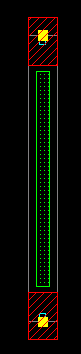
下图是一个tap cell的FRAM View视图。中间绿色的部分是“冗余”的poly。
标签:
asic